As India rapidly transforms into a digital economy, the environmental consequences of accelerated technological adoption have grown impossible to ignore. In FY24 alone, the nation generated a staggering 3.8 million metric tonnes of e-waste, doubling in just a decade and now ranks as the third-largest e-waste producer globally, following China and the USA.
This enormous mountain of discarded electronics is not just a disposal challenge; it is a complex reservoir of untapped economic value, embedded with precious metals such as gold, palladium, silver and copper.
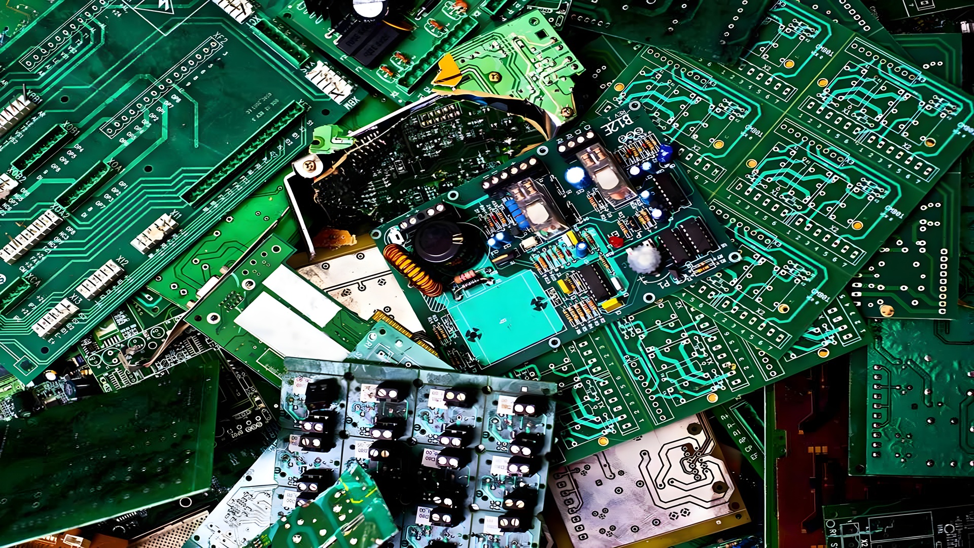
A significant portion of this value lies within obsolete Printed Circuit Boards (PCBs), the backbone of all electronic devices, which are now being recognized as strategic assets in India’s push for circularity. Fuelled by rising urbanisation, disposable incomes, and an insatiable appetite for newer technologies, the surge in PCB scrap has ignited both concern and opportunity in equal measure.
According to the SNS Insider Report, the PCB e-scrap recycling market, valued at USD 699.43 million in 2024, is projected to nearly double and reach USD 1371.12 million by 2032, growing steadily at a CAGR of 8.78%. Such forecasts reflect a compelling market trajectory that aligns economic incentives with ecological responsibility.
To harness the full potential of PCB recycling, state-of-the-art processing lines which comprises tailored shredders, granulators, hammer mills, and highly efficient separation systems including magnetic and eddy-current separators can be utilized to recycle all kinds of PCBs, such as the computer boards, cell phone boards, TV boards, copper-clad laminate, and other household appliances, and the separation of leftover material of the mixed metal and nonmetal materials.
The Multi-Stage Process of Printed Circuit Board Recycling
The comprehensive recycling journey for PCBs commences with the systematic collection of discarded units. This initial phase is then seamlessly followed by an organized system of sorting and meticulous dismantling, utilizing established methodologies to prepare the material for subsequent processing.
Here is a detailed, step-by-step elucidation of the recycling process:
Collection: This foundational step involves the methodical gathering of end-of-life PCBs from various sources such as discarded consumer electronics, industrial machinery, communication devices, and household appliances. These sources include obsolete computers, smartphones, televisions, and printed circuit boards found in larger electronic assemblies.
Sorting: Once collected, the PCBs undergo categorization based on their specific type, size, and intrinsic material composition to optimize downstream processing.
Dismantling and Separation: In this phase, the PCBs are broken down, and their various constituent components are carefully segregated. This can involve both manual and automated methods to separate larger elements.
Material Treatment and Recovery: The now-separated components proceed to specialized processing stages where different materials (e.g., metals, plastics, fiberglass) are subjected to specific treatments for their extraction and purification.
Reprocessing and Reusing: Finally, the high-purity materials recovered from the treatment phase are reprocessed as needed and prepared for reintegration into new manufacturing cycles, thereby reducing the need for virgin raw materials and minimizing environmental impact while promoting a more sustainable and circular economy.
The Importance of Shredders in PCB Material Recovery
A crucial component of the PCB recycling process is the shredder, which plays a vital role in the mechanical separation of materials. The PCB shredder efficiently breaks down PCBs into smaller pieces, making it easier to separate the different materials.
By reducing the size of the PCBs into more manageable pieces, the shredding operation boosts the efficiency of subsequent separation stages by increasing the surface area accessible for metal recovery. Additionally, the shredding process assists in the elimination of non-metal components, thereby streamlining the overall recycling procedure. With the capability to segregate mixed metal and nonmetal components with up to 99% purity, PCB recycling plants that utilize robust PCB shredders can transform discarded circuit boards into high-purity metal, fibre, and resin outputs.
As we move towards a circular future, the PCB recycling industry presents a lucrative opportunity for recyclers while positioning India as a leader in sustainable e-waste recovery and reuse, effectively converting waste into economic treasure.
Gallery